Intel asserts it is the industry leader in packaging technologies for semiconductors, which today have expanded capabilities that enable the most demanding AI compute applications used in the cloud and data centers.
Packaging is well understood in the semiconductor manufacturing field as being distinct from chip design, but the two are closely related in the overall field. Intel has years of experience at both sides of the manufacturing process, but it is lately promoting its packaging prowess as a differentiator as it promotes its overall ability with Intel Foundry in its renewed appeal to find fab customers in addition to using its fab to create its own chips. CEO Lip-Bu Tan renewed support for Intel Foundry at Intel Foundry Direct Connect last week in a keynote address to nearly 1,000 customers and partners.
Packaging prowess will be a key differentiator for Intel Foundry in its bid to out-do TSMC and Samsung, said Jack Gold, an analyst at J. Gold Associates. “Intel already is leading in packaging,” Gold said in an interview at Direct Connect in San Jose, Calif. “If Intel can continue to leverage packaging, it’s a good option for them.”
Gold estimated half the cost of a $2,000 chip is due to the packaging required. In that sense, he believes packaging ingenuity is “more important” that a chip’s process node design.
And Navid Shahiari, executive vice president of packaging and test at Intel Foundry Technology and Manufacturing, told reporters that packaging superiority will be more important to Intel and its customers, as well as the entire industry, in the next 10 to 15 years, especially compared to the past decade.
“We have the most complete portfolio of advanced and associated processes and backend testing. We want to the be the OSAT [Outsourced Semiconductor Assessment and Test) of choice for customers,” Shahiari said.
He explained that a customer building a high-performance computer or other device will be able to use an 18A process node from Intel or one from TSMC “or any silicon and we will do advanced packaging on a silicon fab somewhere else.” Intel will be able to do die testing, yield improvement support, assembly and test. “If a customer approaches us with any need from package design to simulation modeling, we have all the capabilities and design to work with them on our processors—every engineering discipline to support their needs.”
For all of Intel’s positioning itself as the industry’s packaging leader, one analyst at Gartner demurred. “Leader here is very subjective,” said Gartner analyst Gaurav Gupta in comments to Fierce. “Intel has the technology and offerings, but TSMC has much higher customer traction. Intel is trying to push itself with more offerings in advanced packaging to compete with TSMC and showcase for its potential customers the variety of options they can choose.”
To its credit, Intel is open to customers using Intel advanced packaging even if they don’t want the Intel silicon, Gupta noted.
“At this point, Intel is still trying to learn the foundry way of doing the business and it’s not a secret that Intel’s foundry is bleeding money and they will try to attract customers in all possible ways,” Gupta said. In fact, Intel recently reported a $2.3 billion operating loss for its foundry business in the first quarter, flat compared to the previous quarter. Revenue in the quarter jumped by 7% year-over-year to $4.7 billion on the strength of internal wafer shipments. The losses were attributed to structural cost pressures and startup costs connected to ramping up Intel 18A.
But Gupta agreed with Intel and others that advanced packaging will be even more critical in the future. “It makes sense for Intel to market itself well,” he said. “They have a hard task to convince customers that are already working with TSMC. It isn’t just about technology leadership but a service mindset, being able to fulfill demand on time and being flexible to customer demand.”
Intel basically competes with TSMC and Samung in leading edge silicon and packaging in the foundry space. “They must gain customer trust,” Gupta said. “To be better they need to have a better technology offering, potentially lower cost, or an ability to help customers get their products to market faster. Ideally it would be all three as they are looking for new customers, which is a hard task.”
Intel currently is present in the US and EU with a potential to provide silicon diversity, which matters more in the current tariff environment. “But they still need to execute, which is where they have been lagging in the past decade or so,” Gupta said.
So what in the world is advanced packaging?
While chip design is focused on creating integrated circuits, packaging refers to the physical enclosure, connections and mechanics needed for a chip to operate and interact in a server or other computing system. Engineers must select the right packaging materials, and design a physical layout to connect the chip to other functions as they evaluate thermal properties of materials, signal integrity and ways to protect components from power surges or heat and other influences.
Chip designers work on the functionality of a chip, while packaging focuses on the physical environment and connectivity of the chips and other components. Electronics engineers usually design chips, while packaging is handled by engineers with specialties in semiconductor packaging.
The world of packaging technologies has grown tremendously in recent years, with the introduction of chiplets and heterogeneous integration, blurring the lines between design and packaging,
Importantly, packaging impacts performance, power consumption and size of a system.
One key advantage Intel Foundry has pointed to with packaging is the ability to use an embedded bridge technology to allow other packaging technologies from potential competitors. Called Embedded Multi-die Interconnect Bridge-T (EMIB-T), it can be used for memory connections like HBM4 and UCIe at 32 GB.
At Direct Connect, Intel also emphasized its ability with Foveros and, in development, Foveros 2. Both are advances in 3D chip stacking. Foveros allows face-to-face die stacking, while Foveros 2 is a refinement that reduces the size of bump pitches to sub-10 microns, which greatly increases the density of interconnect. A bump pitch is also known as a solder bump and the pitch is the spacing of these individual bumps that are used for interconnecting a chip and substrate. Bump pitch is critical in dictating density and performance of electronics.
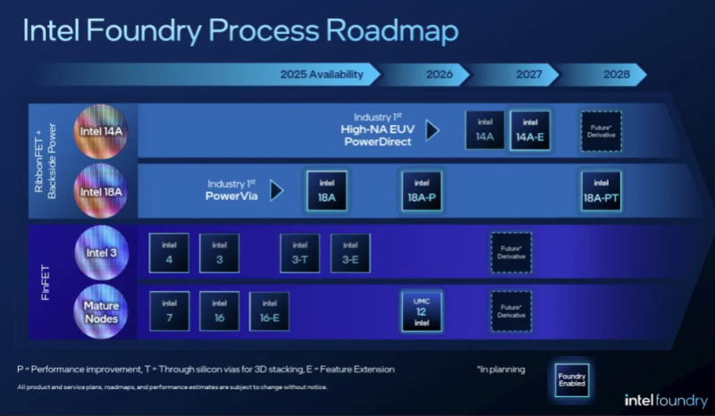
While Intel Foundry promotes its advanced packaging prowess it is also reminding customers of the relationship to its advanced processors, including availability of 18A with the industry first PowerVia later in 2025 and an 18A-PT coming in 2028 with the P and T referring to a Performance improvent and Through silicon vias for 3D stacking.
A industry-first High-NA EUV PowerDirect 14A processor is expected in 2027. The company released this summary chart of its roadmap at Direct Connect: